Last year, I ran a competition to find my next “Strike Force” interns. Max Goldberg and Claire Adair won the competition, and joined me at Abundance 360 as special correspondents. In this blog, you’ll learn key insights from A360 on the materials engineering revolution, as written by Max and edited by Marissa Brassfield.
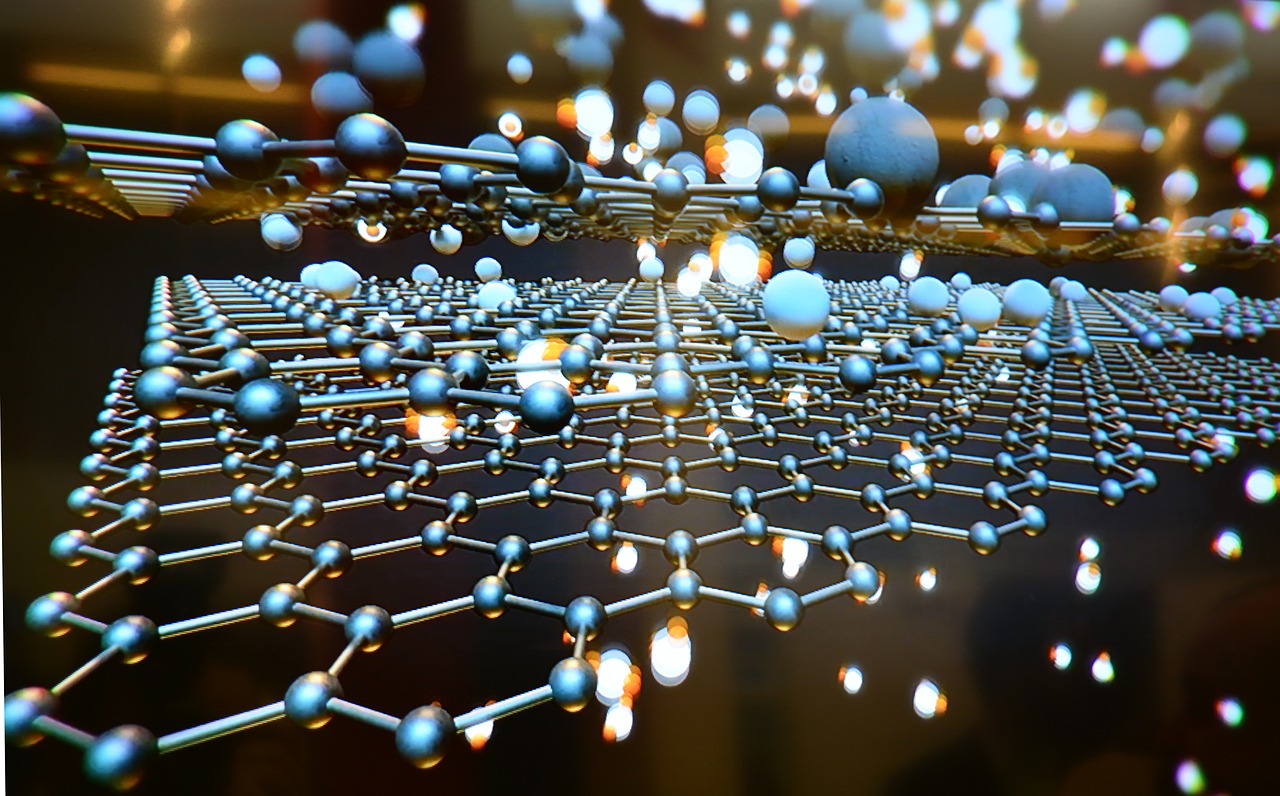
We are in the midst of a materials science revolution that will impact every field of technology in every aspect of our lives.
This year at Abundance 360, Peter brought Om Nalamasu, the CTO of Applied Materials, to share his perspective on how materials engineering is converging with other exponential technologies to enable surprising breakthroughs.
Before we dive in, some background on materials science.
As the Draw Shop video above notes, materials science breakthroughs are accelerating for two reasons:
- Discovery: New tools like the Materials Genome Project, which leverages machine learning to accelerate discovery.
- Engineering: New fabrication tools are allowing precise atomic arrangements that dictate shapes, geometries and sizes.
P.S. Send any tips to our team by clicking here, and send your friends and family to this link to subscribe to Abundance Insider.
Driving Data and Computation
Over 70 years ago, John Bardeen, Walter Brattain and William Shockley sparked the semiconductor revolution with the fabrication of the first transistor.
This fundamental technology now powers every aspect of science, innovation, and society.
Projections place the world semiconductor industry revenue to reach nearly $500 billion in 2018.
Nearly all of today's products and cutting-edge technologies -- from lab testing equipment to technology teams’ Slack channels -- have hundreds of run-ins with the materials science genius that is the transistor.
Let’s look at the integral role semiconductor materials science continues to play in the global computation, Artificial Intelligence, and big data industries.
The Economist magazine predicts that AI-related products and innovations will add nearly $16 trillion to the GDP by 2030.
“Data to this century is what electricity was in the previous generations,” said Nalamasu. “Today, [we generate] something like 230 million tweets per day, 300 billion emails are sent per day, and about a hundred terabytes of data are loaded on Facebook every day. This pales in comparison to what is going to happen in the next five years. The data rate growth is about 80 percent.”
Worldwide data storage capacity is estimated to be around 6 zettabytes by 2020 -- each byte of which is powered by semiconductor materials science.
Exponential network and computation technologies (i.e. Artificial Intelligence, IoT, blockchain technology, autonomous vehicles, the internet) are expected to generate orders of magnitude more data over the next five years than our current storage capacity.
The IoT network alone -- which is projected to consist of over 50 million devices in 2020 -- will generate 600 zettabytes of information. That’s 100x our current storage capacity of 6 zettabytes.
Once it’s collected, how will we make sense and process this data?
The answer: advances in computational materials.
Materials breakthroughs, both in today's semiconductor technologies and tomorrow's quantum computers, are necessary to meet our growing data storage and computation needs.
We’ll definitely need breakthrough materials to meet these enormous big data and computation needs… The exponential nature of Moore’s law is converging with breakthroughs in materials discovery and production…
Machine Learning & Materials Discovery
Traditional materials science involves costly, in-lab iteration and theory-based guesswork.
By harnessing the power of supercomputers, quantum mechanics, and importantly machine learning, materials engineers can do in hours what used to take weeks, months or years.
To contextualize this acceleration, let’s look at Thomas Edison’s invention of the light bulb.
Edison required a bulb with low heat production, low power consumption, and a long-lasting, light-emitting material.
With intuition and empirical data as his guide, Edison set out testing over 1,600 materials. After 14 months of testing and tinkering, he settled on carbon-coated cotton thread.
Fast forward 30 years, and the introduction of the tungsten filament to the market wiped out Edison’s carbonaceous-cotton filament.
In hindsight, Edison’s 1,600 experiments worth of guesswork produced a sub-optimized solution that was readily replaced within three decades.
Modern-day materials engineers, however, can work with materials discovery software to analytically derive and virtually test an optimal new material for a specified application.
“Materials engineering is the ability to detect a very small particle -- something like a 10-nanometer particle on a 300-millimeter wafer,” explained Nalamasu. “That is really equivalent to finding an ant in the city of Seattle.”
Thanks to machine learning and exponential leaps in computation and quantum theory, the high price of guesswork involved in materials discovery is rapidly being phased out in favor of analytical and numerical methods.
The materials scientist of tomorrow will specify materials’ desired properties and some basic processing parameters, and a quantum-computer based machine learning program will return the optimal material composition by crunching accumulated data and solving complicated quantum physics equations.
Materials innovation leads to exponentially more materials innovations.
Remember: supercomputers (and soon quantum computers) are the lineage of the computational materials disruption that’s been taking place for the past 70 years.
Augmented Reality and Virtual Reality
Think back to the state-of-the-art mobile phone in the 1980’s. Big, bulky, and reserved for the Wall Street executive, phones ran upwards of $4,000 and weighed over a dozen pounds. The phones could only be used for calls, and lacked any memory to store contact information.
“If you were to build a smartphone in 1980,” Nalamasu explained, “that would cost something like $110 million. It would be about 14 meters tall, and it would require about 200 kilowatts of energy… that’s the power of materials engineering.”
Today, thanks to materials science breakthroughs in semiconductor technology, touchscreen displays, and batteries, children and executives alike can access smartphones with a 6+ inch OLED (Organic Light Emitting Diode) touchscreen displays, 256+ gigabytes of storage, integrated 1080p cameras, and endless other features.
By the end of 2018, we’ll have over 2.5 billion smartphones in use, according to projections.
Let’s extrapolate the user interface moment for mobile devices allowed by materials science breakthroughs to the current state of Augmented Reality and Virtual Reality.
Today, bulky, expensive, and hard-to-use Virtual Reality headsets dominate the industry.
VR headsets are ripe for precisely the same types of materials breakthroughs that enabled the smartphone era.
Some of the materials breakthroughs anticipated to come in and accelerate VR technology:
- OLED display advances that allow headset resolution to increase from 500 pixels per inch to 3,000+ pixels per inch
- Optics will move from today’s traditional structures to thin films on the order of nanometers in thickness
- Memory improvements to store large Virtual Reality graphics files
- Energy efficient processors and graphic cards will enable better, faster performance
- Battery advances to power the large energy requirements of running high-quality graphics
The future of Augmented Reality and Virtual Reality lies in sleek, slim, lightweight, and beautiful headsets that seamlessly integrate with our day-to-day lives. Thanks to coming materials advances, our future devices will be cheaper, thinner, faster and more powerful.
Also read: TOP 50 MOON SHOTS
WHAT IS ABUNDANCE INSIDER?
This email is a briefing of the week's most compelling, abundance-enabling tech developments, curated by Marissa Brassfield in preparation for Abundance 360. Read more about A360 below.
WANT MORE CONVERSATIONS LIKE THIS? - JOIN ME
At Abundance 360, Peter's 360-person executive mastermind, we teach the metatrends, implications and unfair advantages for entrepreneurs enabled by breakthroughs like those featured above. We're looking for CEOs and entrepreneurs who want to change the world. The program is highly selective. Apply now for Abundance360 Summit if you'd like to develop an Abundance mindset.
Know someone who would benefit from getting Abundance Insider? Send them to this link to sign up.
P.S. I've just released a podcast with my dear friend Dan Sullivan called Exponential Wisdom. Our conversations focus on the exponential technologies creating abundance, the human-technology collaboration, and entrepreneurship. Head here to listen and subscribe.
Topics: Materials Science